Pr
eliminary
P r e l i m i n a r y
February 2001
KM4270
Dual, Low Cost, +2.7V and +5V,
Rail-to-Rail I/O Amplifier
Product Brief
Features at 2.7V
I
160
µA supply current per amplifier
I
4.9MHz bandwidth
I
Output swings to within 20mV of either rail
I
Input voltage range exceeds the rail by >250mV
I
5.3V/
µs slew rate
I
35mA short circuit output current
I
24nV/
Hz input voltage noise
I
Directly replaces MAX4126, OPA2340, LMV822,
and TLV2462 in single supply applications
I
Available in SOIC and MSOP package options
Applications
I
Portable/battery-powered applications
I
PCMCIA, USB
I
Mobile communications, cellular phones, pagers
I
Notebooks and PDA's
I
Sensor Interface
I
A/D buffer
I
Active filters
I
Signal conditioning
I
Portable test instruments
General Description
The KM4270 is a dual ultra-low cost, low power,
voltage feedback amplifier. At 5V, the KM4270 uses
only 160
µA of supply current per amplifier and is
designed to operate from a supply range of 2.5V to
5.5V. The input voltage range exceeds the negative
and positive rails. The KM4170 (single) and KM4470
(quad) are also available.
The KM4270 offers high bipolar performance at a low
CMOS price. The KM4270 offers superior dynamic
performance with a 4.9MHz small signal bandwidth
and 5.3V/
µs slew rate. The combination of low power,
high bandwidth, and rail-to-rail performance make
the KM4270 well suited for battery-powered com-
munication/computing systems.
© 2001 Fairchild Semiconductor
Corporation www.fairchildsemi.com
Patents Pending
Outperforms the competition in
single-supply applications at a
lower cost!
Advertised 5V
KM4270
Competitors
Units
Specifications
A
B
C
D
G = 1 BW
4.3
5
5.5
5.6
6.4
MHz
Noise
27
22
25
24
11
nV/
Hz
Slew rate
9
2
6.0
2
1.6
V/
µs
Supply current
160
850
750
250
550
µA
Available Packages
Ordering Information
Part No.
Package
Container
Pack Qty
Eval Bd*
KM4270IC8
SOIC-8
Rail
95
KEB006
KM4270IC8TR3
SOIC-8
Reel
2500
KEB006
KM4270IM8
MSOP-8
Rail
50
KEB010
KM4270IM8TR3
MSOP-8
Reel
4000
KEB010
Temperature range for all parts: -40°C to +85°C.
* Evaluation boards are available to aid in the evaluation of these products. See the full
data sheet or website for complete information.
-
+
-
+
1
2
3
4
Out1
-In1
+In1
-V
s
+V
s
Out2
-In2
+In2
8
7
6
5
SOIC
-
+
-
+
1
2
3
4
Out1
-In1
+In1
-V
s
+V
s
Out2
-In2
+In2
8
7
6
5
MSOP
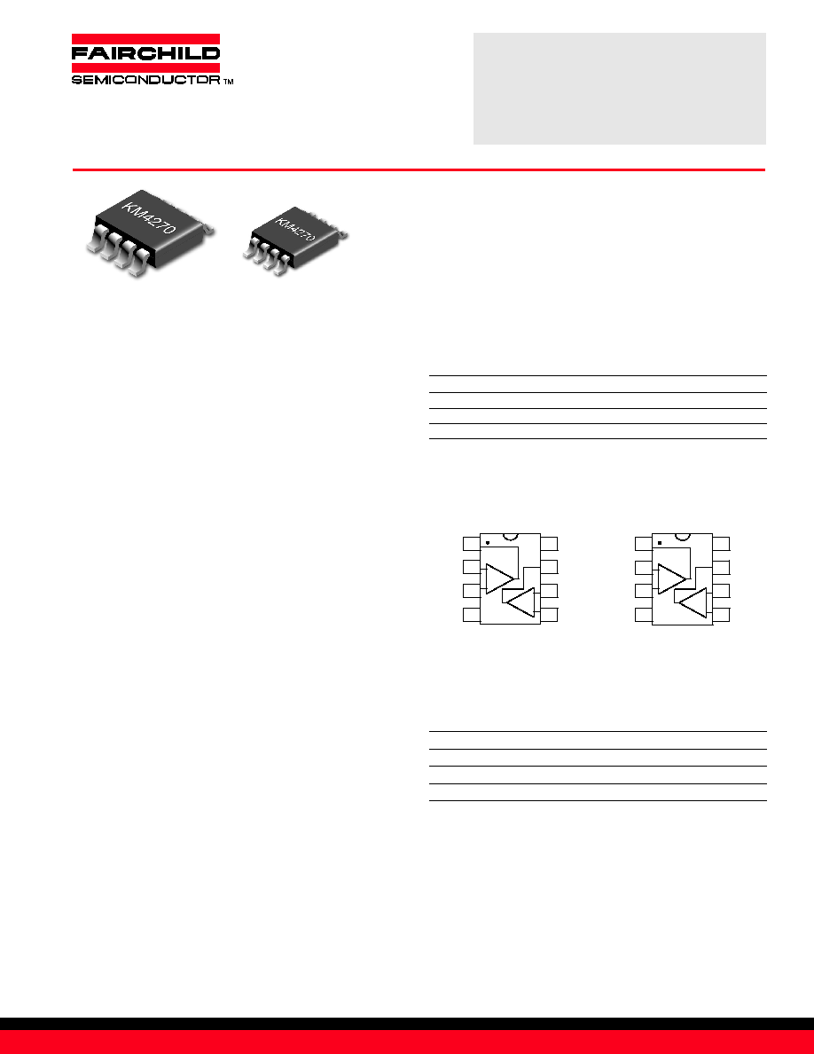
MSOP-8
(not actual size)
SOIC-8
(not actual size)
Pr
eliminary
KM4270
Typical Specifications
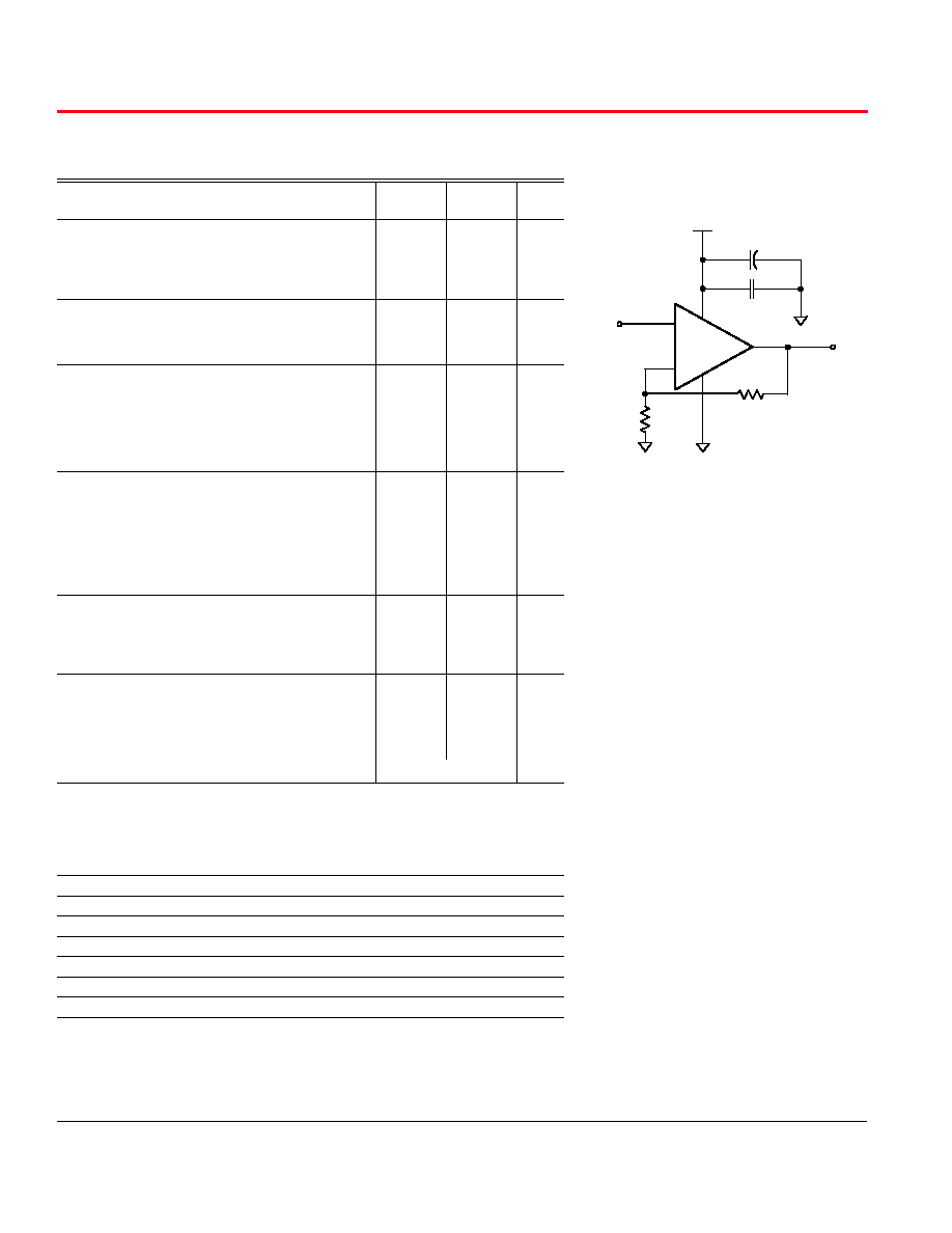
Typical Circuit
Configuration
+
-
KM4270
R
f
0.01
µF
6.8
µF
Out
In
+V
s
+
R
g
LIFE SUPPORT POLICY
FAIRCHILD'S PRODUCTS ARE NOT AUTHORIZED FOR USE AS CRITICAL COMPONENTS IN LIFE SUPPORT DEVICES OR SYSTEMS WITHOUT THE EXPRESS WRITTEN APPROVAL OF THE PRESIDENT
OF FAIRCHILD SEMICONDUCTOR CORPORATION. As used herein:
1.
Life support devices or systems are devices or systems which, (a) are intended for
surgical implant into the body, or (b) support or sustain life, and (c) whose failure to
perform when properly used in accordance with instructions for use provided in the
labeling, can be reasonably expected to result in a significant injury of the user.
2.
A critical component in any component of a life support device or system whose failure
to perform can be reasonably expected to cause the failure of the life support device or
system, or to affect its safety or effectiveness.
Lit No. 600312-001
Electrical Characteristics
(G = +2, R
f
= 5k
, R
L
= 10k
to V
s
/2, T
a
= +25°C, unless noted)
PARAMETERS
CONDITIONS
TYP
TYP
UNITS
Vs = +2.7V
Vs = +5V
Frequency Domain Response
2
-3dB bandwidth
G = +1, V
o
= 0.02V
pp
4.9
4.3
MHz
G = +2, V
o
= 0.2V
pp
3.7
3.0
MHz
full power bandwidth
G = +2, V
o
= 2V
pp
1.4
2.3
MHz
gain bandwidth product
2.2
2.0
MHz
Time Domain Response
rise and fall time
1V step
163
110
ns
overshoot
1V step
<1
<1
%
slew rate
1V step
5.3
9
V/
µs
Distortion and Noise Response
2nd harmonic distortion
1
1V
pp
, 10KHz
-75
-73
dBc
3rd harmonic distortion
1
1V
pp
, 10KHz
-76
-75
dBc
THD
1
1V
pp
, 10KHz
0.03
0.03
%
input voltage noise
>10KHz
24
27
nV/Hz
input voltage noise
>2KHz
32
28
nV/Hz
crosstalk
10KHz
TBD
TBD
dB
DC Performance
input offset voltage
0.5
1.5
mV
average drift
5
15
µV/°C
input bias current
90
90
nA
average drift
32
40
pA/°C
power supply rejection ratio DC
83
60
dB
open loop gain
90
80
dB
quiescent current per amplifier
136
160
µA
Input Characteristics
input resistance
12
12
M
input capacitance
2
2
pF
input common mode voltage range
-0.25 to 2.95 -0.25 to 5.25
V
common mode rejection ratio
DC
81
85
dBc
Output Characteristics
output voltage swing
R
L
= 10k
to V
s
/2
0.020 to 2.68 0.04 to 4.96
V
R
L
= 1k
to V
s
/2
0.05 to 2.63
0.07 to 4.9
V
R
L
= 200
to V
s
/2
0.11 to 2.52
0.14 to 4.67
V
output current
16
30
mA
short circuit output current
35
60
mA
recommended power supply operating range
2.5 to 5.5
V
Notes:
1) For +5V supply, a 2V
pp
condition was used.
2) For G = +1, R
f
= 0.
Absolute Maximum Ratings
supply voltage
0 to +6V
maximum junction temperature
+175°C
storage temperature range
-65°C to +150°C
lead temperature (10 sec)
+300°C
operating temperature range
-40° to +85°C
input voltage range
+V
s
+ 0.5V, -V
s
- 0.5V
ja
for 8 lead SOIC
152°C/W
ja
for 8 lead MSOP
206°C/W